

Strain Gauge Fundamentals
How do I calculate material stress from strain? How can I select the right strain gauge and install it correctly?
Read More
In the course of our daily lives, we have to place trust on the reliablitiy of electronic components integrated in cars, smartphones, airplanes, and countless other devices. In many of these products printed circuit boards (PCBs) are integrated. The reliability of complex electronics and overall electrical systems is a result of experienced development and intensive testing.
PCBs are exposed to mechanical and thermal impacts not only during their manufacturing process, but also during their transport and in action (for example: deformation, misuse, vibration, shock, thermal exposure).
During the manufacture of PCBs, the following malfunctions and stresses may occur:
During transport and operation, the following impacts could lead to a malfunction:
All these effects can lead to a complete failure of components. If a systematic failure of a PCB is detected too late, the fulminating costs would be massive.The costs would continue to increase, as long as the detection of the malfunction is delayed. The rule of 10 shows that the later a systematic failure of a new product is detected, the costs per defect unit multiply by a factor of 10.
Based on the fact that detecting systematic failures at an early stage of development is absolutely essential, OEM manufacturers have increasingly begun to request their suppliers to check the mechanical quality of PCBs.
The utilization of PCBs has increased in recent years due to the following reasons:
International associations such as IPC (Association Connecting Electronics Industries) and JEDEC (Joint Electron Device Engineering Council) – 9704 have been established, and these provide guidelines describing where, how and wherewith strain measurements on PCBs have to be performed.
Many companies have created their own test procedures to ensure that all manual handling steps are executed correctly during the assembly as well as developed test scenarios for PCB testing to cover all relevant cases.
Numerical simulation methods such as FEA are limited in their scope since they are based on mathematical model approaches. Therefore, physical tests on real PCBs are at least additionally required to test the real strain behavior of the board. Other test methods such as CTs and X-rays are not sufficiently adequate to check the influence of the mechanical impact and are, on top of that, expensive methods to employ.
Strain values are the only reliable calculations for measuring the mechanical deformation of PCBs. Therefore, strain gauges are designated to measure the deformation of the PCBs to an extremely accurate degree. PCBs are usually small in dimension, and the challenge is to install strain gauges in the limited space available.
HBK offers over 2000 different strain gauges for special applications, alongside some specialized strain gauges for PCB strain measurement. The RF91 three-grid miniature rosette, for example, is an excellent product to measure strain on miniature components such as PCB since the direction of principal strain is unknown. Moreover, it is only 5mm in diameter and can, therefore, be mounted easily on PCBs. It is available in different variants: prewired and with integrated solder pads. Other strain gauges, such as the RY31-3/120 (6.9mm diameter), can also be used for PCB testing.
Start your measurement right away with the PCB Test Kit. From the matching strain gauges to the measuring bridge amplifier and the data acquisition software, the kit includes everything you need for strain measurements on PCBs in compliance with IPC/JEDEC 9704.
From the sensor to the result, simply “plug and measure”:

The tension status on PCBs is mostly unknown and mechanically complex. Strain situations result in the deformation of a plate. Plate deformation does not follow the classic models of beam deformation or torsion of a shaft, which are quite accurately described by linear mechanical statics.
Furthermore, it needs to be considered that an assembled PCB contains several single components that are soldered or connected in different ways to the PCB. This means that a PCB is quite heterogeneous in its material properties.
It is neither useful nor possible with respect to cost and time to check every single section of a PCB according to the strain properties and behavior. Therefore, measurements on PCBs are set at areas where the risk of failure is estimated to be especially high such as:
QuantumX is a modular, freely scalable and distributable data acquisition system from HBK for measurement and testing purposes allowing quicker innovation. All modules offer an Ethernet interface and can be freely combined with each other. All channels work completely time synchronized - module to module with < 1 µs.
Every channel can be individually parameterized via software, supporting the following:
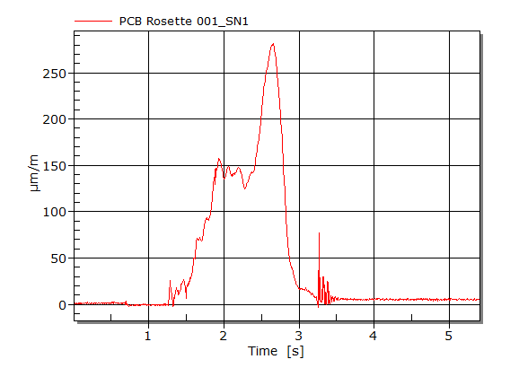
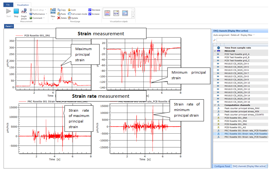
With the HBM DAQ software catman AP, it is easy to set up a PCB board strain measurement. A quick and easy visualization of data is one of the strengths of catman. Data recording can be performed differently using trigger or special time points.
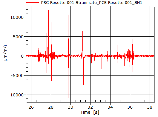
The three measurement grids of the RF91 rosette allow the calculation of maximum and minimum principal strain (rates) as well as the corresponding angles. The latest versions of catman also support strain rate measurement (the strain is derived from the time).
In the subsequent steps, the way to set up a strain rate measurement in catman is shown:
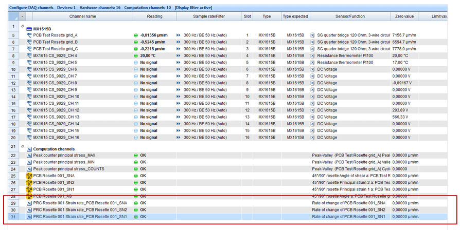
1. Open the catman software and check the relevant channel of the strain gauge. The green lights indicate that the channel is detected and is ready for measurement. In this example, the three grids of the rosette are connected with Channels 1, 2, 3.
")
2. Use the sensor database to assign the channels to the sensor application. In this case, drag and drop the 3 wire 120 Ω strain gauge to each of the three active strain channels.
")
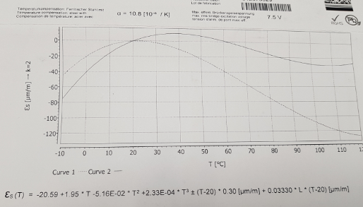
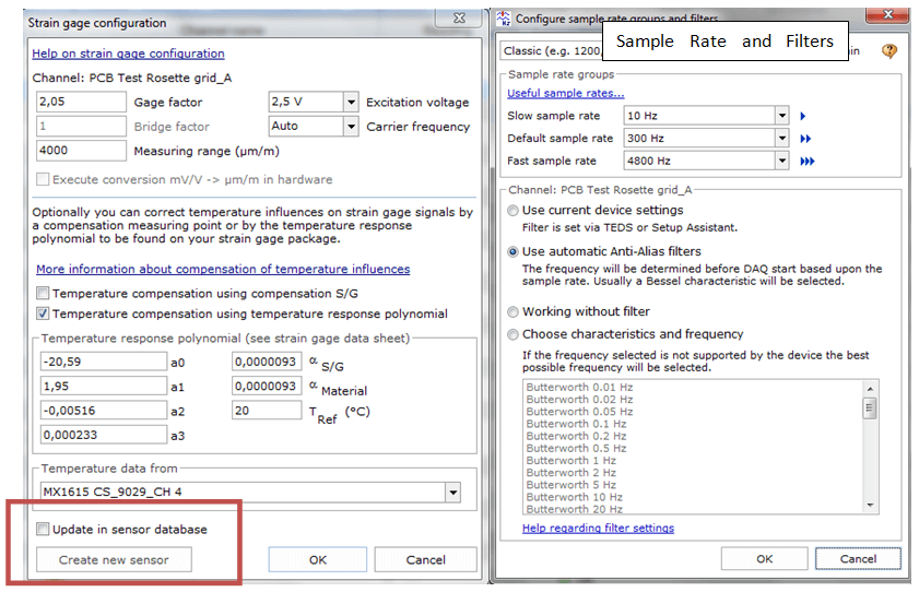
1. Now, the sensor specifications need to be set. Set the correct parameters by using the k-factor displayed on the datasheet of each HBM strain gauge package. Enter the excitation voltage, the bridge factor, and the measurement range. Also ensure that you look at the temperature compensation polynomial if you want to correctly consider the temperature fluctuation material properties.
2. Set the sample rate (classic or decimal) and filters correctly before beginning measurements. Click on ‘Create new sensor’ and activate ‘Update in sensor data base’ to save your parameters in the database.
3. Select all channels and zero the offset of the strain channels of the rosette. The zeroed strain channels appear.
1. Now, we have to set up the rosette calculation channel. A new channel needs to be created, and catman makes it easy for the user to create different setups for rosette calculations.
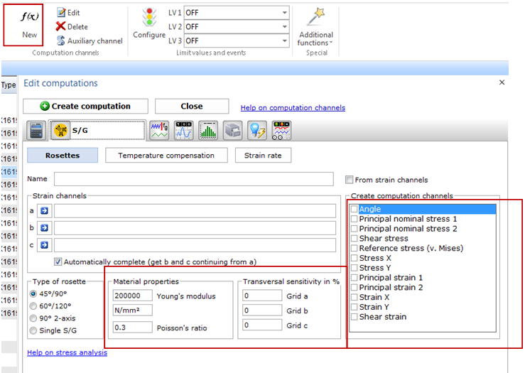
2. Add all three channels in a, b, c and define the material properties and the transverse sensitivity of the gauges. Choose the right rosette type (0/45 or 60/120 for the three grid rosettes) and select the relevant strains (principal strain, shear strain).
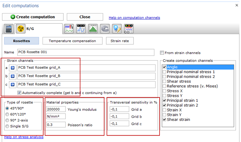
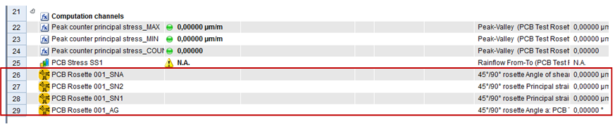
3. Click on ‘Create calculation’. Now, the calculated channels appear in the channel list.
4. Set a name and click on ‘Apply changes’
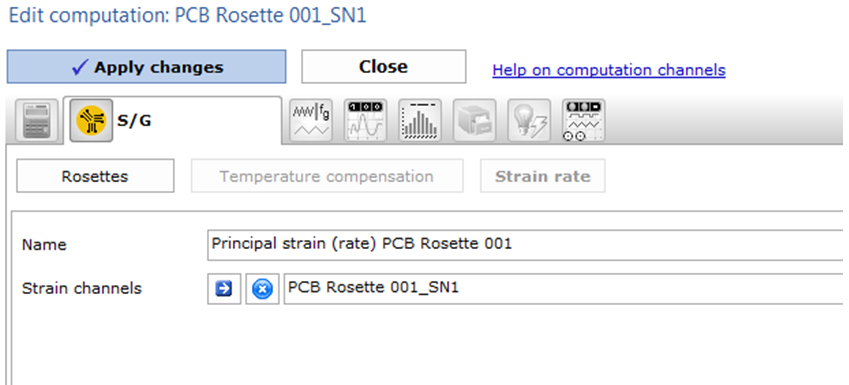
5. The strain rate channels will appear in the ‘computation channel’ list at the end.
Go to ‘Visualization’ and configure your own GUI
catman®AP from HBK is a powerful software package for PC based data acquisition and data analysis. Thanks to an intuitive user interface, you are only a few clicks away from starting your measurement. Simply configure the amplifier using TEDS, the transducer electronic data sheet, or the extendible sensor database – and the test can start.
Many options for graphical data analysis and versatile export options make catman®AP a reliable and indispensable tool for every measurement technician.
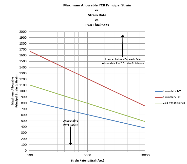
The aim of the analysis is to check if the measured data meets the acceptable criteria for the PCB strain. The following diagram illustrates the boundary lines as a function of the strain rate and the board thickness according to IPC / JEDEC-9704A (2012).
The idea is that the maximum principal strain (Y-axis) should not exceed a certain value. With increased PCB thickness higher principal strains are acceptable. Additionally, another criterion needs to be considered – the strain rate. This means that the lifespan of a PCB is impacted not only by the pure value of the maximum principal strain but also by the speed of changing the strain (impulse). Fast changes in material usually result in earlier micro cracks and material damage.
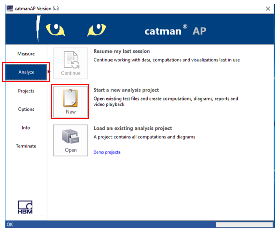
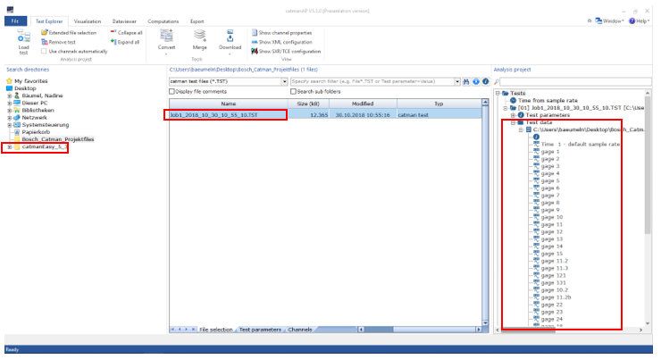
1. To analyze the test data, open a new ‘Analyze’ project in catman.
2. Search for the test data and drag & drop it to the column on the right hand side.
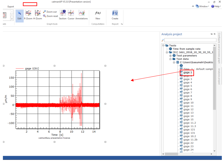
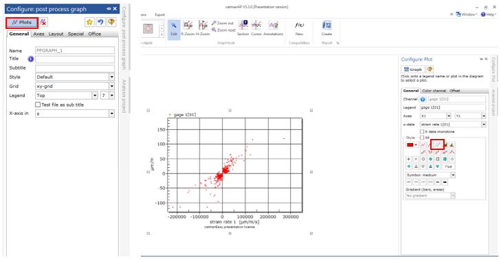
1. Change to the ‘Visualization’ panel. Create a graph by dragging & dropping the test data of gage 1 to the empty surface.
2. Then choose the corresponding strain rate 1 and drag it onto the text gage 1[01] in the graph explanations. Use strain rate 1 as x-axis.
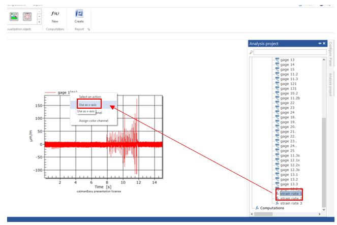
3. The following graph will appear:
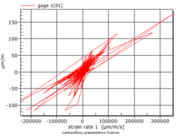
4. As this is not the desired shape of the graph, configure the plot as follows (dotted-style).
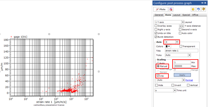
5. Adjust the x-axis by choosing a manual logarithmic scaling.
1. To picture the limit line, define the following data series function (according to IPC/JEDEC-9704):
Max. allowable strain = sqrt[2.35/(PWB thickness)]*[1900-300*log(strain rate)]
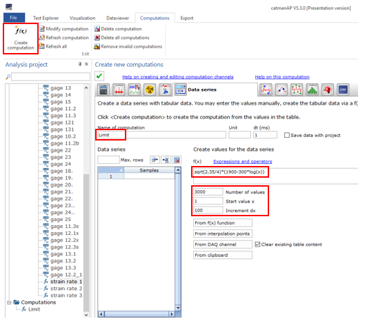
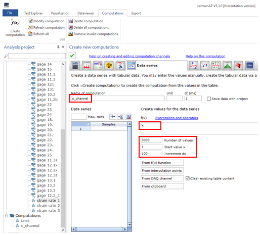
and x as function
1. Finally visualize the computed functions. Drag & drop the ‘Limits’ computation to the displayed graph. Then drag & drop the ‘x_channel’ computation onto the Limits in the graph explanations and use as x-axis.
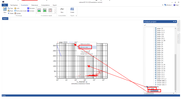
2. The resulting graph looks as follows:
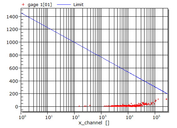
According to IPC/JEDEC-9704 Printed Wiring Board Strain Gage Test Guideline, the measured strain is within the acceptable strain range. The tested PCB is, then, not damaged during the manufacturing process.
Legal Disclaimer: TECH Notes are designed to provide a quick overview. TECH Notes are continuously improved and therefore, change frequently. HBK assumes no responsibility for the correctness and/or completeness of the descriptions. We reserve the right to make changes to the features and/or the description at any time without any prior notice.

This will bring together HBM, Brüel & Kjær, nCode, ReliaSoft, and Discom brands, helping you innovate faster for a cleaner, healthier, and more productive world.
This will bring together HBM, Brüel & Kjær, nCode, ReliaSoft, and Discom brands, helping you innovate faster for a cleaner, healthier, and more productive world.
This will bring together HBM, Brüel & Kjær, nCode, ReliaSoft, and Discom brands, helping you innovate faster for a cleaner, healthier, and more productive world.
This will bring together HBM, Brüel & Kjær, nCode, ReliaSoft, and Discom brands, helping you innovate faster for a cleaner, healthier, and more productive world.
This will bring together HBM, Brüel & Kjær, nCode, ReliaSoft, and Discom brands, helping you innovate faster for a cleaner, healthier, and more productive world.
This will bring together HBM, Brüel & Kjær, nCode, ReliaSoft, MicroStrain and Discom brands, helping you innovate faster for a cleaner, healthier, and more productive world.